


AI Shows Hidden Semiconductor Reaction Pathways
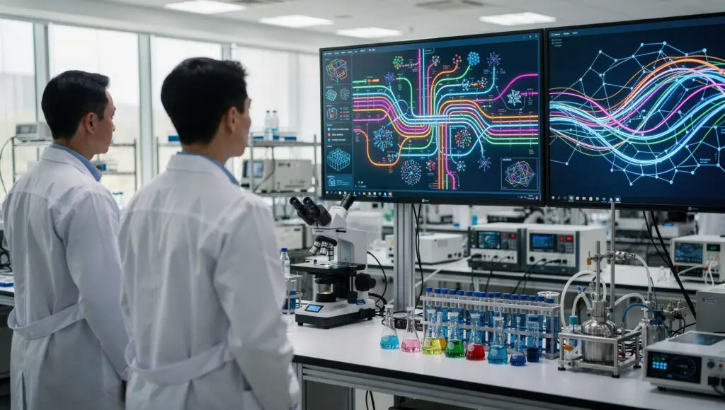
Researchers from DGIST and Sungkyunkwan University made an AI system that makes it easy to see how semiconductor nanocrystals react. Researchers can use the technology to turn complicated chemical reactions into easy-to-understand maps that look like subway systems.
This picture helps scientists understand growth processes that they couldn’t see with just experiments. It greatly lowers the level of uncertainty when looking at how complex semiconductor materials are made.
Quantum Dots Drive Next-Generation Display Innovation
Colloidal quantum dots are semiconductor nanocrystals that let you control how light is absorbed and emitted very precisely. They are important for display technologies that need to reproduce colors accurately because their optical properties change with size.
More and more, global tech companies are using quantum dots to make advanced display panels and visual systems. Their significance is also growing in the fields of infrared imaging and sensor development.
Challenges in Understanding Nanocrystal Formation
Tracking the pathways of nanocrystal formation has been difficult for scientists in the past because reactions are very complicated. Researchers had to rely on inference instead of direct observation because there wasn’t enough experimental data.
This method limited accuracy and made it harder to understand how semiconductors grow. Using standard experimental analysis methods, it was often hard to see complex branching reactions.
Recommended Article: Philippines to Lead ASEAN in Promoting Ethical AI Use
Integrating Transformer AI and Topological Data Analysis
The research group used Transformer-based AI and topological data analysis methods together. This integration enabled AI to automatically reconstruct incomplete reaction data with enhanced structural precision.
The system quickly found links between reaction steps by putting together broken-up datasets. The resulting image shows a full and clear picture of the reaction flow structure.
Finding Many Ways for InAs to Grow
Researchers used an AI model to make indium arsenide nanocrystals for use in infrared semiconductors. The AI showed that there were many branching growth paths instead of just one straight line.
This discovery changed a lot of what we thought we knew about how nanocrystals are made. It gave us a better understanding of the reaction dynamics that affect how well semiconductor materials work.
Role of Additives as Reaction Flow Controllers
The AI analysis indicated that supplementary materials serve as regulatory “traffic lights” during synthesis. These additives have a big effect on the direction of the reaction and the growth of the nanocrystals.
Researchers can better control synthesis if they understand this control mechanism. It makes it possible to change the properties of materials by making smart chemical changes.
Implications for Future Materials Research and Industry
Researchers stressed that AI works like an invisible navigation system that finds hidden chemical pathways. This method greatly improves the efficiency of research and development in the field of semiconductor materials.
The study got international attention thanks to funding from major Korean research programs. The fact that it was published in the Journal of the American Chemical Society shows that it is important to science.